28
2022-07
Specializing in optical products research and production and development of high-tech enterprises
The working principle of the semiconductor laser is the excitation mode, the use of semiconductor material (that is, the use of electrons) in the band transition light, with the cleavage of the semiconductor crystal surface to form two parallel reflection mirror as a mirror, the composition of the resonant cavity, so that light oscillation, feedback, produce light radiation amplification, output laser. Semiconductor laser advantages: small size, light weight, reliable operation, low power consumption, high efficiency.
2022-07-28
27
2024-03
Semiconductor lasers begin to be used in optical fiber communication systems
Therefore, the rapid development of varieties, a wide range of applications, has more than 300 kinds, the main application of semiconductor lasers is Gb LAN, 850nm wavelength of semiconductor lasers for Gh LAN
2024-03-27
27
2024-03
By 1989, the LD with a width of 0.1mm had reached a continuous output of 3.7W.
For example, distributed feedback (DFB) and dynamic single-mode LD for optical fiber communication and optical switching systems, narrow linewidth tunable DFB-LD, visible light waves for information processing technology such as optical discs.
2024-03-27
27
2024-03
There are conduction and valence bands in semiconductor materials
It can also turn the energy of electricity into light, and the width of the forbidden band of the material determines the working wavelength of the optoelectronic device. The development of materials science enables us to use the energy band engineering of semiconductor materials for a variety of exquisite cutting, so that it can meet our various needs and do more things for us, but also to make the semiconductor optoelectronic devices work wavelength breakthrough material band gap width limit extended to a wider range.
2024-03-27
10
2022-01
The working principle of the semiconductor laser is the excitation mode, the use of semiconductor material (that is, the use of electrons) in the band transition light, with the cleavage of the semiconductor crystal surface to form two parallel reflection mirror as a mirror, the composition of the resonant cavity, so that light oscillation, feedback, produce light radiation amplification, output laser. Semiconductor laser advantages: small size, light weight, reliable operation, low power consumption, high efficiency.
2022-01-10
12
2021-11
Semiconductor laser packaging technology is mostly based on discrete device packaging technology.
The role of the package is mainly to protect the die and complete the electrical interconnection. The semiconductor laser package is to complete the output electrical signal, protect the normal operation of the die, output: the function of visible light, both electrical parameters, and optical parameters of the design and technical requirements, can not simply be discrete device packaging for semiconductor lasers.
2021-11-12
12
2021-11
This mainly depends on the quality of the semiconductor material, the die structure and geometry, the internal structure of the package and the encapsulation material, the application requires to improve the internal and external quantum efficiency of the semiconductor laser. The conventional Φ5mm semiconductor laser package is to bond or sinter a square die with a side length of 0.25mm on the lead frame.
2021-11-12
12
2021-11
A square die with a side length of 0.25mm is bonded or sintered on the lead frame. The positive electrode of the die is connected to the gold wire through a spherical contact point. The bonding is that the inner lead is connected to one pin, and the negative electrode is connected to the other pin of the lead frame through a reflective cup. Then the top is encapsulated with epoxy resin. The function of the reflector cup is to collect the light emitted from the side and interface of the die,
2021-11-12
09
2021-11
It is very important to maintain the color purity and luminous intensity. In the past, the method of reducing the driving current was used to reduce the junction temperature. The driving current of most semiconductor lasers was limited to about 20mA. However, the light output of semiconductor lasers increases with the increase of current, and the driving current of many power semiconductor lasers can reach 70mA.
2021-11-09
09
2021-11
Lattice defects and dislocations to improve internal efficiency, at the same time, how to improve the internal structure of the die and package, enhance the probability of photon emission inside the semiconductor laser, improve light efficiency, solve heat dissipation, optimize the design of light and heat sink, improve optical performance, accelerate the process of surface mount SMD is the mainstream direction of industrial research and development.
2021-11-09
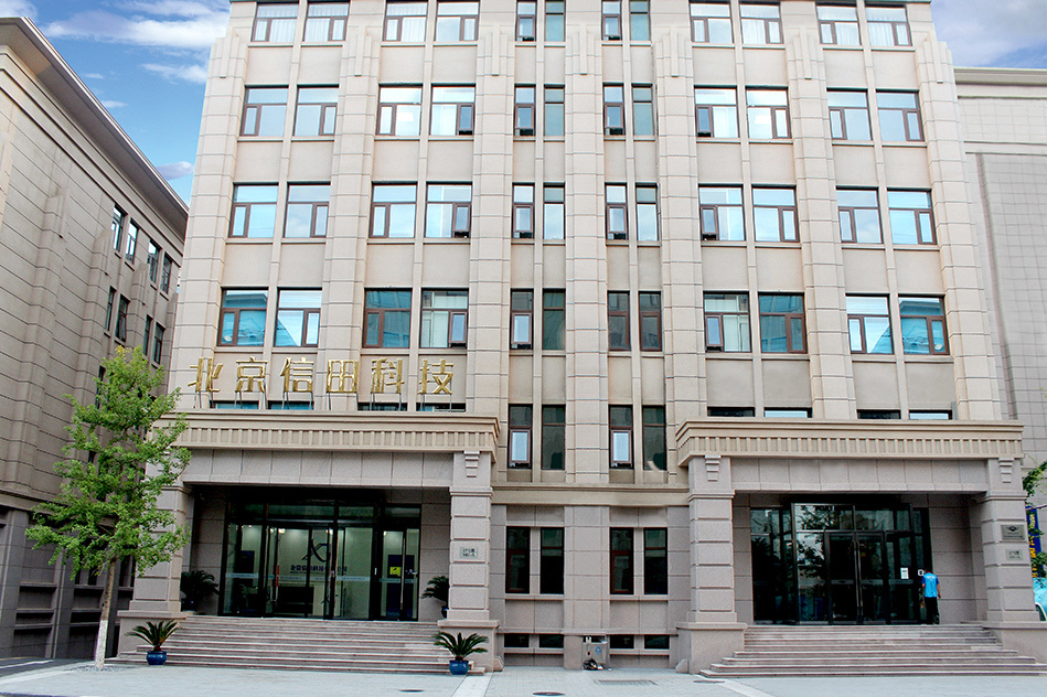
Beijing Xintian Technology Co., Ltd
Address: 102A, Building 27, Yard 2, Huanke Middle Road, U Valley, Liandong, Jinqiao Industrial Base, Tongzhou District, Beijing
Telephone : 0086-10-81314835/57323722
0086 182 1070 6870 (English)
WhatsAPP : 0086 182 1070 6870
Wechat ID : 0086 182 1070 6870
Fax : 86-10-57323723
E-mail : sales@xt-optic.com
wangdi@xintian-tech.com
Contact person : Mr.WangDi

Scan code attention to us
Copyright©Beijing Xintian Technology Co., Ltd

